Laser Etching, Drilling and Cutting of PCBs and Piezo Ceramics

Direct Machining Control enabled the customer to use their laser system for etching, drilling, and cutting of PCBs and piezo ceramics. The customer tried several CAM software packages, but they either didn't support galvo scanner machining or crashed due to large and complex files with dense hatching. Before contacting Direct Machining Control, the user settled to use 4 different software packages to control different parts of the system: galvo scanners, positioning stages, camera, and height sensor. DMC was installed to replace those four different software packages. The process was simplified from complex multiple steps to a single recipe with minimal operator input. The creation of new processes became easy, visual and user intuitive.

Challenge

The customer had a laser machining setup designed for internal prototyping and small-scale production purposes. The intention was to etch, drill and cut PCBs and piezo ceramic wafers.

  • Gerber file import. All the parts are designed in Gerber format. Currently, the user had to export them to DXF and hatch them in CAD software. Then import files to laser marking software.
  • Combining galvo scanners and positioning stages. Processing requires high resolution and accuracy. However, only using positioning stages is not an option, since dense hatching is used, machining with stages would take several days. So, the customer had small field ScanLAB galvo scanners with the telecentric lens mounted over Aerotech positioning stages.
  • Thick wafer drilling/cutting. Wafers are thicker than beam spot waist. In the beginning, the customer used to focus the beam at the bottom and kept scanning with laser marking software at the same height. As alternative laser marking software was used to make a layer, then switching to Aerotech Motion Composer to make Z adjustment and run drilling recipe in marking software again. Both alternatives required unnecessarily long processing times and regular operator input.
  • Wafer flatness correction. Large wafers are not completely flat. This means that the laser focus position doesn't change linearly throughout the wafer. This results either in a non-repeatable machining process or in an overkill while etching and cutting to make sure the wafer is cut all the way through.
  • Double-sided machining. Wafers had to be machined from both sides. Machining trajectories must match existing patterns on both sides within 2 um.
  • Operators had no experience with CNC or other machining processes. Thus, programming machining workflows was time-consuming and inconvenient.

Solution

We analyzed the situation with the customer and made several online sessions to work together on the setup to fully understand their needs. The following solutions were implemented with DMC software:

  • The customer is able to import Gerber and NC Drill files, so there are no longer any intermediate steps. A Gerber and NC Drill file support was developed and added to DMC free of charge. Now the customer can import the same files that are used for parts creation. Moreover, their coordinates are being preserved when importing, so different layers imported with different files match automatically. E.g. holes on PCB are matching the etching patterns perfectly. So there is no need for position adjustment which saves time and helps to avoid errors.
  • Galvo scanner and positioning stages are combined using the Stitching tool in DMC. No need to use additional software for galvo scanners and positioning stages. All motion is divided between galvo scanners and positioning stages automatically (Figure 1).
  • Etching, drilling and cutting processes are combined in the same recipe to save time and maintain accuracy. The single recipe uses several types of Gerber files and NC drill files. Gerber file is hatched and used for etching and cutting, while NC drill file is used for layer-by-layer drilling. Different laser and speed parameters are set for different parts of the recipe to perform them efficiently. I.e. PCB is drilled with two sets of parameters, one for the copper top and bottom and one for the polymer middle layer (Figure 2).
  • The user is using a coaxial camera positioned by galvo scanners. The camera and laser focus height matches almost perfectly. So DMC camera Autofocus tool is used to find laser focus position (Figure 3). A special tool was developed to create height maps by measuring the focus position on the wafer in various positions. After that, the fabrication recipe is automatically transformed to match the height differences on the sample. Alternatively, a Keyence height sensor might be used for better measurement accuracy.
  • DMC integrated Machine Vision is used for visual alignment to compensate for the wafer displacement before the start of processing and after flipping the wafer for machining of the other side.
  • The entire design of the recipe and control of the processing is made in a single software window using visual tools and no G-Code programming. This saves a great amount of time and nerve for the user.
  • Keyence height sensor is used to measure and display etching results. The operator can see and log machining results like depth of ablated areas accurately without taking the wafer away.
Figure 1. Several Gerber and NC Drill files imported to DMC software and different settings are selected for different processes.
Figure 2. Grey stitching lines where the object is split for galvo and stages machining are visible. Different object colours represent different laser and speed parameters.
Figure 3. The camera view is used to find camera and laser focus position automatically.
Figure 4. The camera is used for alignment on the PCB.
Figure 5. Height-map acquired with Keyence sensor and matched with machining trajectories. The customer uses this feature for quality inspection and result logging.

Results

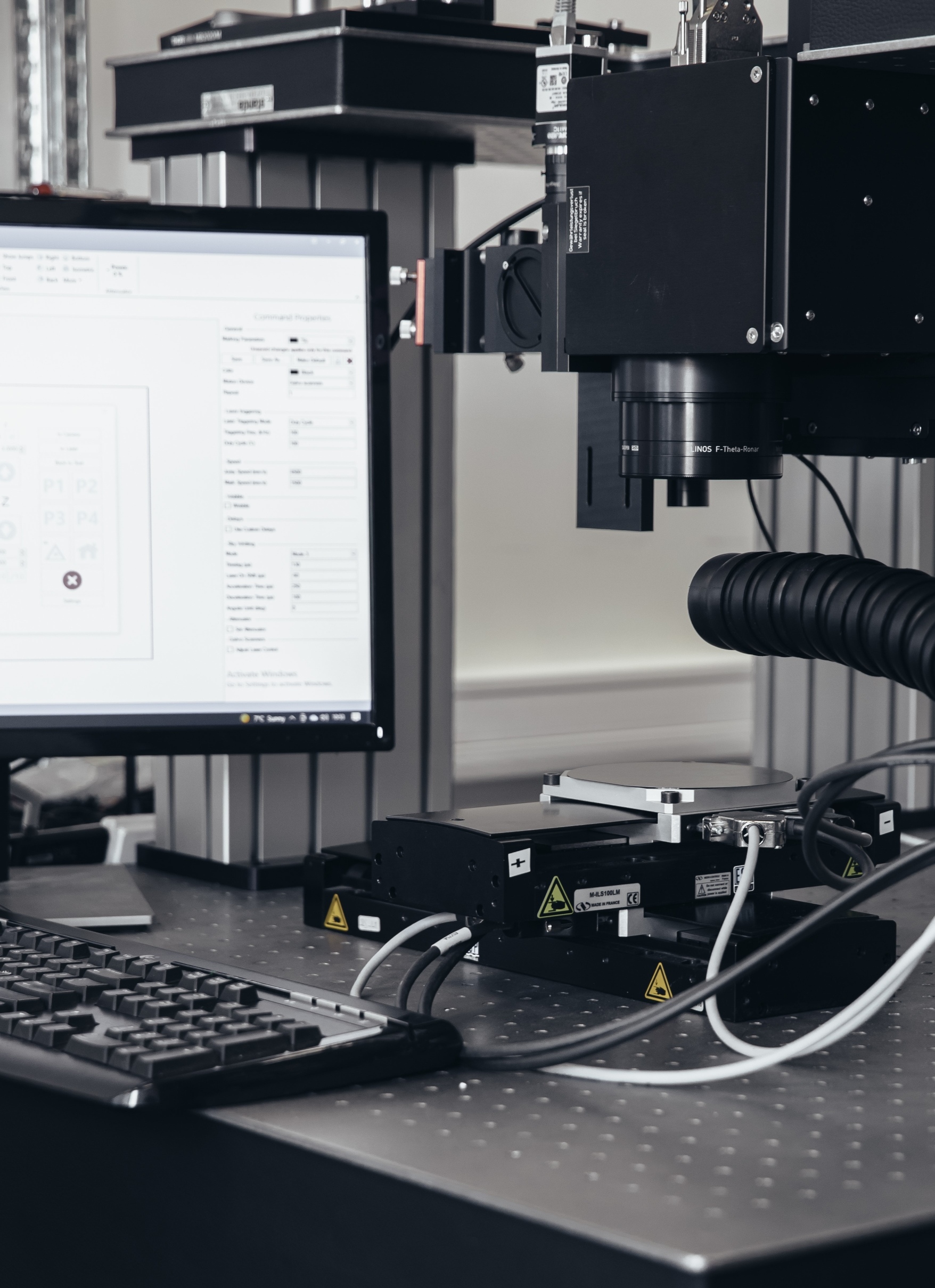
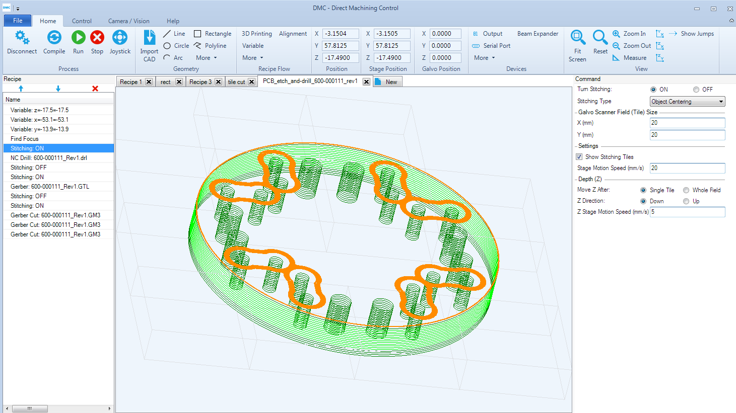
Using DMC laser machining software, customer is finally able to use their setup for intended purposes: etching, drilling and cutting of PCB and piezo ceramics wafers. All processing is achieved by a single recipe. Double-sided wafer processing is enabled using automatic visual alignment.

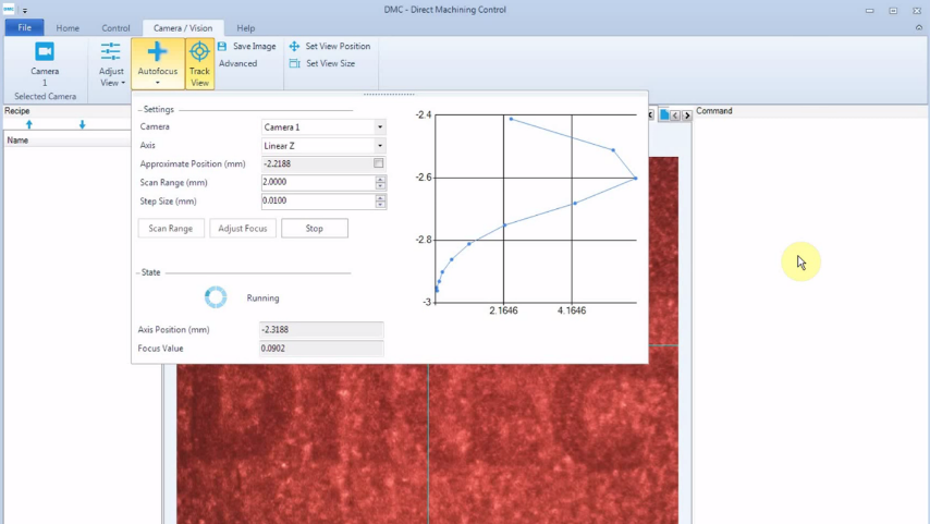
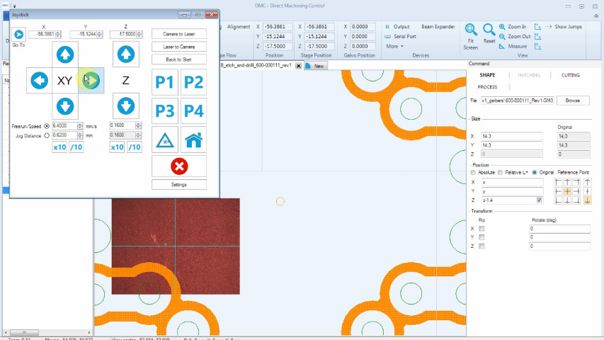
Accuracy, speed and process repeatability is achieved by combining galvo scanners and stages and by measuring and compensating wafer flatness variations.

All of it is done in a single software window in a visual and intuitive way, without any kind of programming.